4DSP’s New FPGA-based Products Benefit from Xilinx UltraScale
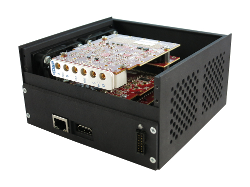
4DSP is using the newest and most powerful g eneration of Xilinx FPGAs in its most recent products. The basic logic cell structure of these UltraScale devices remains essentially unchanged and the available resources on the chip are largely what you would expect – LUTs, Memory, DSP blocks, standard IOs, and SerDes transceivers. Xilinx has, however, fine-tuned these resources specifically for the increasingly demanding applications that designers face. As a close partner of Xilinx, 4DSP immediately began developing products to take advantage of the performance gains offered by these new devices and we introduced our first UltraScale-based product in December. 4DSP now offers Kintex UltraScale FPGAs on our three newest PCIe boards.
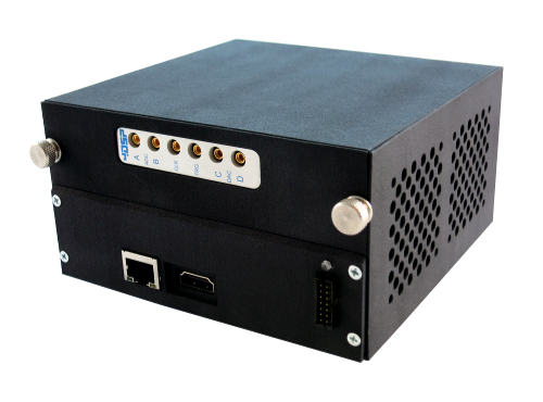
PC820 – carrier card with 1x FMC (VITA 57.1) site
PC821 – carrier card with 2x FMC (VITA 57.1) sites
PC870 – one 10-bit A/D ch. at 5Gsps and one 10-bit D/A ch. at 5Gsps
UltraScale FPGAs are designed for applications that require massive I/O and memory bandwidth, huge data flow, and excellent DSP and packet-processing performance. The 20nm UltraScale architecture provides a number of advantages over Xilinx’s previous highest-end Kintex-7 and Virtex-7 28nm FPGA families, the largest of which are capable of holding the equivalent of up to 20 million ASIC gates. UltraScale offers a significant performance boost over this with the equivalent of 50 million ASIC gates, while reducing power consumption. The design also addresses the scalability limitations of system throughput and latency, and it improves communication, clocking, and critical paths to accommodate greater data flow. UltraScale also offers more and faster interconnects to minimize the bottleneck to silicon performance at advanced nodes. The increased number of routing resources improves handling of the large amount of data that current high-speed SerDes can deliver to these programmable devices.
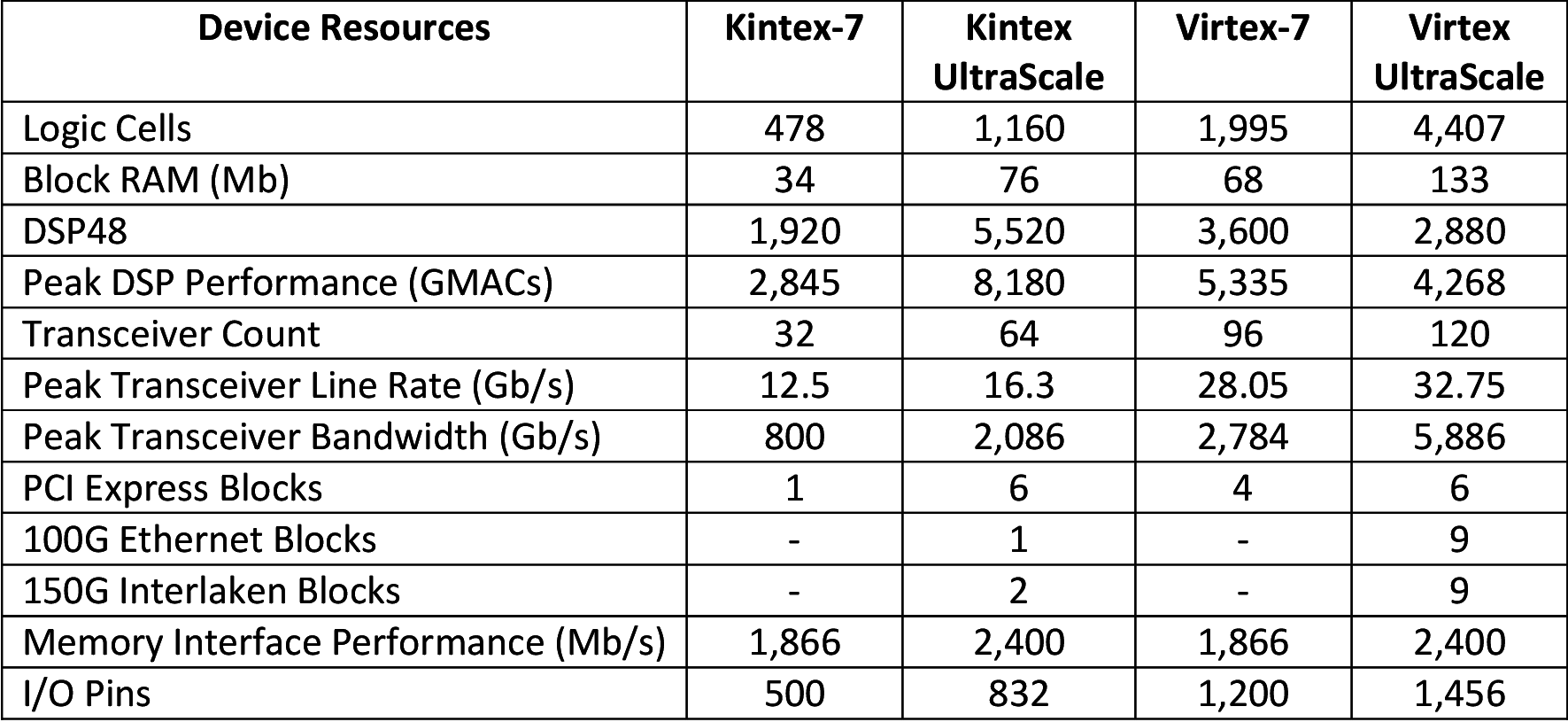
Comparison of the Maximum Values of 20nm and 28nm Devices (Xilinx)
The revamped clocking architecture on UltraScale chips uses a multi-region scheme reminiscent of ASIC designs. In this way, Xilinx greatly reduces the large portion of a clock period that is lost to skew. UltraScale devices additionally now support higher-resolution clock gating to enable ASIC-like power conservation. This results in higher-frequency operation, a reduction in timing problems caused by skew, lower power requirements, and higher overall bandwidth.
Working hand-in-hand with UltraScale devices is Xilinx’s Vivado Design Suite, an integrated design environment developed to support these newer, high-capacity FPGAs. Vivado is an IP and system-centric software tool that reduces the amount of time necessary to design programmable logic and I/O. It is a ground-up rewrite of their older design tool, ISE. 4DSP’s own StellarIP firmware design tool and proven reference design library supports both Vivado and ISE and can be used to automatically create compatible projects. StellarIP is part of the Board Support Package (BSP) included with all 4DSP FPGA-based boards and FMCs. The BSP also includes the 4FM GUI (multifunction test, monitoring and measurement tool) and the Data Analyzer (real-time digitized data and spectrum display tool).
4DSP is developing more new products that feature UltraScale processing, including a more advanced version of our popular CES720 (Compact Embedded System). These will be announced later this year, so keep an eye out here and in our press area for new developments.